Pattern deposition
(Photolithography process)
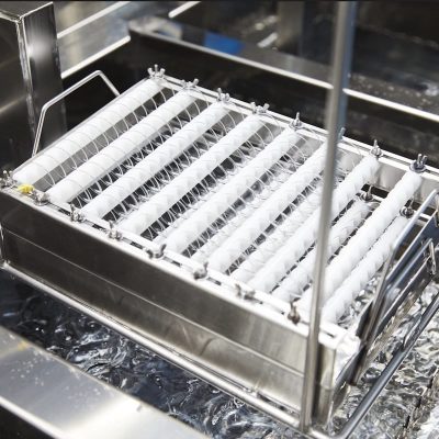
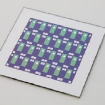
Precision patterning can be achieved using photoresist and lift-off or etching. Feature sizes down to 3 µm can be achieved, depending on the type of coating required.Furthermore, depending on the conditions, a size of 1 μm is also possible. ①Work environment/Equipment We will manufacture filters/mirrors with high-precision patterns in combination with various deposition technologies. Super clean room ISO class 1 [Process Flow] *Equipment introduction Maximum supported size: Φ6in / Maximum substrate thickness: 25mm (Include prism) ②Pattern accuracy (Dichroic film L/S) Accuracy up to L/S = 1 μm is possible ③Boundary accuracy (A faint outline) Comparison with metal mask (our comparison) ④Pattern example 1)Dichroic coat/shading film …
Metal sputter film
Substrate size, Film forming material, and features that can be deposited W160×L325×H110(mm) *Maximum effective area for Al+SiOx film. Since there is very little heat damage to the workpiece, it can be uniformly and firmly applied to resins such as PC, PET, PBT, ABS, PMMA, COP, COC, glass, metal, silicon wafers, three-dimensional objects, and lenses. Al, Ag, Cr, NbO, Ti, Au, Cu, Pt, Pd, Rh, Ru, W, Ge, Hf, Ta, Mg, Mo, Si, Sn, Zn, Zr, Ni, Fe, etc. typically becomes a metal film Typical oxide film forming material include NbOX, TiOX, Al2O3, HfO2, Ta2O5, SiO2, and ZrO2. Quality evaluation A B C reflectance:450nm 89.2 88.0 88.8 reflectance:700nm 89.24…